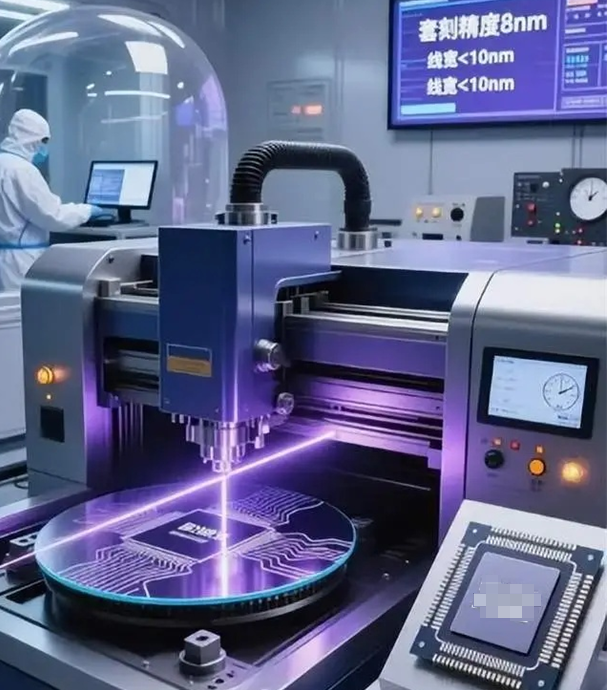
Out on the packaging line, a 0.3°C drift in bake temperature is all it takes to turn a promising Mini LED run into scrap—dead pixels, delamination, and yield loss that shows up right where you hate to see it: the rework bin. You need heat that lands exactly where it should, every single cycle. What matters, technically We built this lamp around NIR infrared heating with sub-millimeter thermal uniformity. The thermal field across the chip array hits the intended profile without hot spots or cold edges. Repeatability is baked into the control loop. Setpoints hold tight across shifts, and the system keeps the same thermal budget cycle after cycle. That gives you consistent soft bake and hard bake behavior on the photoresist—no over-curing, no under-setting that invites patterning risk. Why it works in this process Mini LED chip packaging needs clean, controlled thermal steps—inside Class 1–100 cleanroom constraints. This lamp runs with zero particle generation during operation, so you’re not fighting contamination on the wafer or compromising package integrity. It stays stable for 24/7 operation, keeping output consistent through high-throughput lithography and packaging sequences, while energy use stays inside the process window. The payoff is tighter critical dimension control, fewer reworks, and cycle times you can plan around. Here are the practical details NIR infrared heating is fast and precise, but it’s sensitive to emissivity differences across substrates and to line-of-sight geometry. Plan the lamp position and dwell profile to match your chip layout. Make sure the mounting and thermal isolation fit your equipment envelope. Once it’s aligned, the process window tightens—and becomes far more repeatable.