August 20, 2026
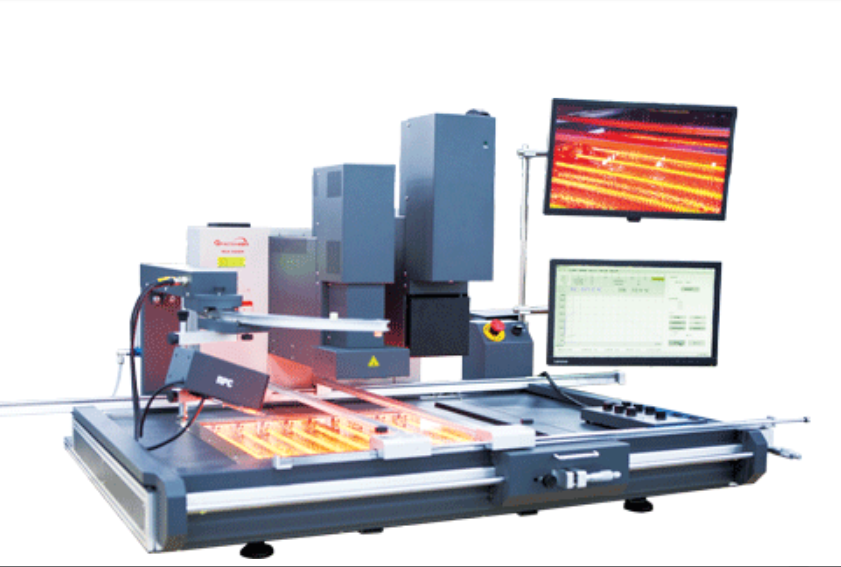
Finding the Hottest and Coolest Locations on a Mixed PCB
Large copper areas, heat sinks and high-mass packages often heat slowly, while small dark bodies and exposed edges may heat quickly. The actual extremes depend on the board layout and oven field, so they must be measured. Create a risk map showing copper distribution, package mass, shields, connectors, edges and airflow. Instrument the likely extremes at relevant solder interfaces. Include a vulnerable component even if it is not the hottest point. Repeat the profile from a controlled starting state and during steady production.
A three-pass location study
- **Predict:**select locations from layout, mass and material evidence.
- **Challenge:**rotate or reposition an engineering board to separate a product-fixed pattern from an oven-fixed field.
- **Confirm:**repeat the final sensor set through cold start and steady production. If the source of the pattern remains uncertain, rotate or reposition an engineering board to distinguish product-fixed behavior from an oven-fixed field. Report the ramp, time spent in relevant bands, peak temperature and cooling response at every location rather than a single average. Use the confirmed map to select Goldisgood active length, pitch and zones from the documented emitter range, then profile again. Related: zone power and speed and profiling after maintenance.