Why We’re Swapping Old Ovens for IR Curing in the Fab
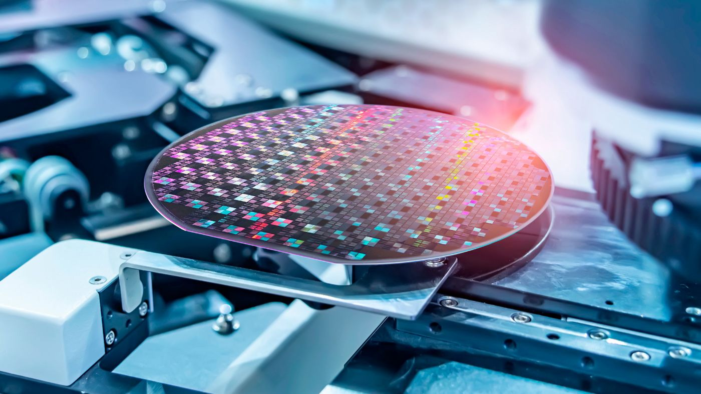
Let’s be honest: those old-school convection ovens are a bit of a dinosaur. In the semiconductor world, we’re seeing a huge shift toward certified infrared (IR) curing lamps. It’s not just about following the “green” rules or hitting lead-free mandates—it’s about the fact that they actually work better. Here is the thing about convection. You’re basically heating up a giant box of air just to get your wafer warm. It’s slow, it wastes a ton of power, and you’re always worrying about dust or particles floating in that hot air and landing on your work. IR is different. It’s direct. The energy goes straight from the lamp to the substrate. No middleman. No waiting around for a massive chamber to warm up. You hit the switch, the photons hit the material, and it turns into heat instantly. It’s fast. Really fast. And that means you’re using way fewer kilowatt-hours per wafer. Then there’s the “lead-free” headache. If you’re working with lead-free solders or polymers, you’re dealing with higher melting points and a very tiny window of error. If you overshoot the temp by even a little bit, you’ve just fried your substrate. That’s why we use short-wave and medium-wave IR. It gives us a dial for the heat penetration. You can cure the surface perfectly without soaking the entire component in heat. No warping, no thermal stress, just a clean cure. But, there is a catch. These lamps put out an incredible amount of heat in a very small space. You can’t just slide one of these into an old oven and call it a day. If you don’t have the right exhaust and cooling fans to handle those sudden heat spikes, you’re going to melt your own housing. You have to plan for the cooling side of things just as much as the heating side. We design these systems to replace those clunky, outdated thermal processes. By getting rid of all that air-handling junk, you drop your carbon footprint and keep the environmental inspectors happy. It just makes sense.